Petes images and diagrams compiled
You should print the main PCB and Opamp diagrams and use them as mark sheets so when you are soldering your unit together, you can mark them off one by one on the printouts with pen or flouro pen.
I usually scan the ACTUAL PCBs I receive and print them out as well to be ultra sure that all information match with the actual PCB. So that means I would have 3 print outs as mark sheets which are the Excel BOM, the main PCB diagram and the scan of my actual PCBs. It’s a longer process but it helps me identify if I have soldered the wrong components somewhere by going through these 3 stages of confirmation marking.
Very Rough Schematic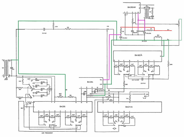
Sourced: lazpro.com/84rough.jpg
Main PCB diagram
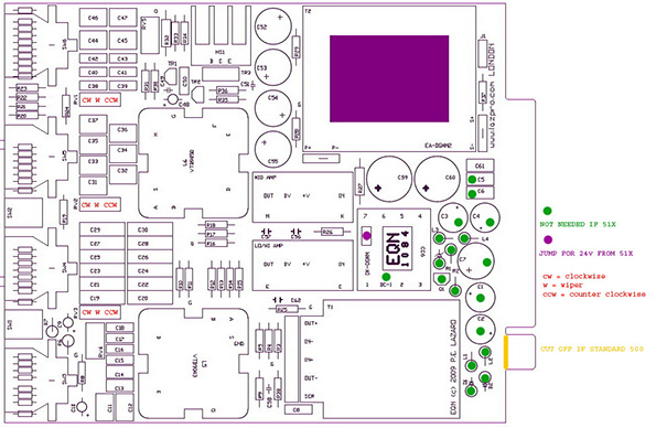
Sourced: lazpro.com/xinf.jpg
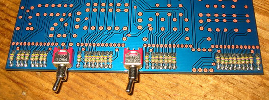
The *FIT UNDERSIDE with the fluoro green dots in the Main PCB diagram refers to soldering the
– 33 X 4M7 Miniature resistors (R39 to R71) and
– 2 X toggle (rocker) switch (SW1, SW2)
underneath the main PCB like in the pic below.
Sourced: lazpro.com/mr.jpg
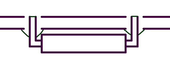
Also trim the leads(legs) of the resistors protruding from the underneath side of the main PCB board when you are done soldering it. I presume you are also trimming the legs of the toggle switch. Can someone message me to confirm this?
Sourced: lazpro.com/minires.jpg
OP Amp PCB diagram
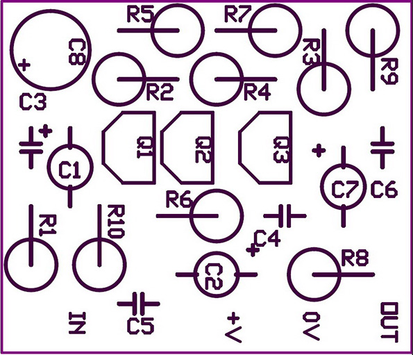
Sourced: lazpro.com/ampol.jpg
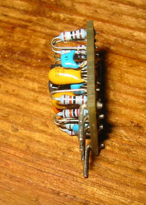
Sourced: lazpro.com/bend.jpg
“The pins need to have a fairly close-up bend to the pcb.
The easiest way is to solder them in and then bend them.
Don’t worry about roughing up the surface… it’ll give extra grip in the sockets.”
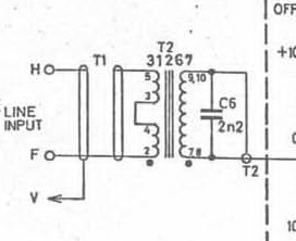
Sourced: lazpro.com/itx.jpg
“As you can see… the input transformer needs to be wired 4:1… primaries in series and secondaries in para.
2 goes to IN+
5 goes to IN-
7&8 go to OUT+
9&10 go to OUT- Ground”
Hairball EA-1166 Output Transformer arrived and well packed!
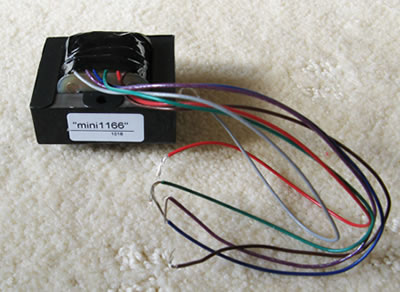
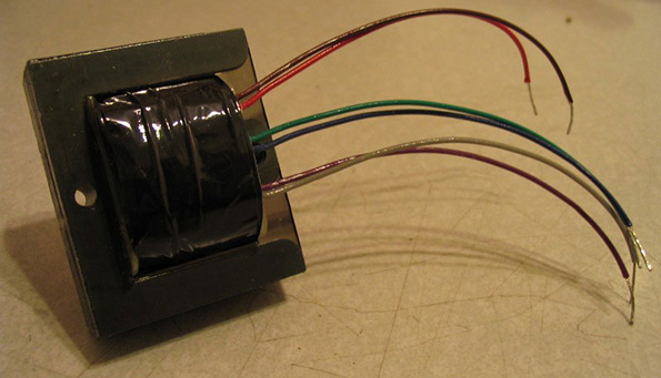
Sourced: Hairball Audio
Wiring: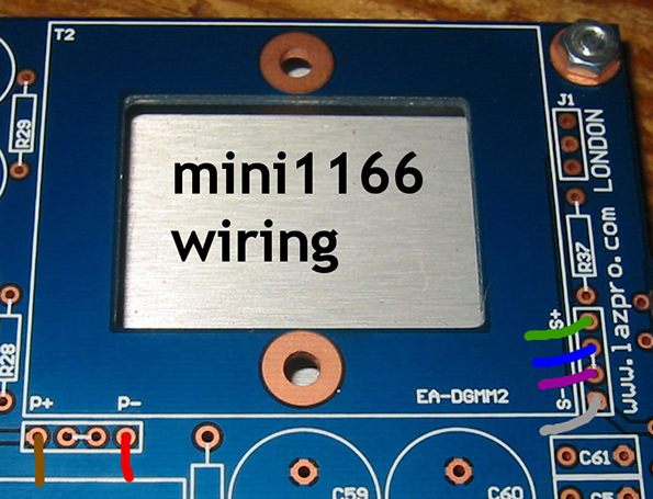
Sourced: Hairball Audio
Bottom of pic:
P+ = Brown
P- = Red
Right side of pic:
S- = Grey
Next to S- = Violet
S + = Green
Next to S+ = Blue
PCB scans for mark off sheets or reference.
(Right Click link and save to download)
EQN 2009 PCB scan-normal – click here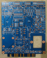
EQN 2009 PCB scan-invert – click here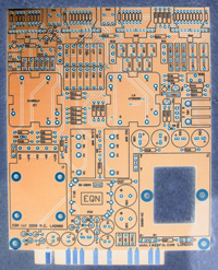


Feedback
*To embed code in Feedback, insert code between "pre" tags.